
ONGOING PROJECTS
- Development of Remote Radiation Detection Imaging System Mounted on a Drone
- High Resolution SPECT using Variable Pinhole Collimator
- Positioning Algorithm for CZT Virtual Frisch-grid Detector
- Multi-purpose Super-resolution Gamma Detector
- Multi-pinhole SPECT
- Low Profile Light Guide using Diffusion Film
- Advanced Reconstruction for Radiation imaging (ARRA)
COMPLETED PROJECTS
- Reconstruction of Dose Distribution in In-beam PET for Carbon Theraphy
- Image Registration for Breast Cancer Study
- High Energy Collimator Design for I-131
- Plasma-Display-Panel based X-ray Detector (PXD)
- CCD based Gamma Camera
- Abdomen Registration for PET/CT and MR images
- Performance Optimization by Patient Dose Analysis and Image Quality Assessment in CT Fluoroscopy
- Cone-beam based system matrix for a pixelated SPECT detector
- Development of Time-of-Flight Method for Improvement of Signal-to-Noise Ratio
Plasma-Display-Panel based X-ray Detector (PXD)
Introduction
Screen-film-based radiography is being rapidly replaced by direct digital radiography (DR). DR is a convenient and cost effective device that can be used to create and store the medical low dose X-ray images. Amorphous silicon (a-Si)-based indirect acquisition and amorphous selenium (a-Se)-based direct acquisition systems are usually used to detect the X-rays. For the indirect DR, the X-ray to charge conversion is achieved by the combination of columnar type scintillators and PIN diodes or CCD, while the equivalent function for the direct DR is performed by a-Se, which is a common material used in this type of DR. Both types of DR detectors require a large number of charge storage device arrays to collect the charges of each pixel. The most widely used charge storage element in DR systems is thin-film-transistor (TFT) array, and this device also assumes a critical role in active-matrix liquid crystal display (AMLCD) panels. Another well-known display device, used in flat panel TVs, is plasma display panel (PDP). Because this device does not require the presence of TFTs in its pixels, its cell structure and manufacturing process is relatively simple. Moreover, the cell structure of a PDP is similar to the conventional micro gas chambers which consist of electrodes and gas-filled volume. Recently, some research groups showed that the cell structure of PDP, which consists of electrodes and gas mixture, could be utilized in the manufacture of radiation detectors.

Fig. 1. Detection scheme and prototype panel of PXD
We defined the x-ray detection and signal generation scheme of a plasma display panel based x-ray detector (PXD) as described in figure 1. Based on the Monte-Carlo simulation studies, the cell structure and gas-mixture have been optimized to enhance the signal-to-noise ratio (SNR) of the PXD. A 5-inch PXD panel consisting of (1 mm × 1 mm × 2.8 mm) cells has been designed and produced, and its intrinsic sensitivity and signal-to-noise ratio have been reported. This prototype detector panel has row and column strips, and it can thus be utilized as an imaging detector. To achieve the 2D x-ray image from the developed panel, a PXD dedicated driving and data acquisition scheme has been designed.
Methods and Materials
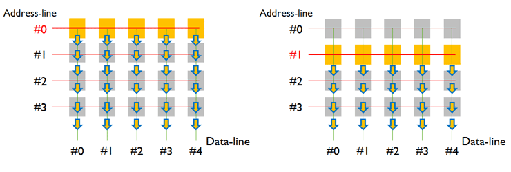
Fig. 2. Line scan readout scheme of PXD. The arrow represents the flow of charge in each pixel.
The scheme of line scan readout system for PXD has been represented in figure 2. Because of the pixel does not have any charge storing elements inside, the charge of each pixel should be read line by line during the x-ray exposure. While an address-line is activated, the charge of each pixel which is connected to this address-line, can be read by multi-channel data acquisition system through each data-line. Then, the address-line is deactivated, and the next address-line is activated. As shown in figure 2, the proposed DAQ system consists of a multi-channel high voltage switching board, a multi-channel DAQ board, and an FPGA based control board. High voltage line switching board selects which address-line to be activated. By doing the activation and deactivation of address-line sequentially, the charge of entire detector area can be scanned. The amount of charge which has been collected by the anode in each pixel is measured by multi-channel DAQ board. These two switching and DAQ board are controlled by FPGA board. The information of digitized charge for each pixel sent to PC by FPGA based RS-232 communication, as well. As described in figure 3, the prototype system has a compact design to be easily utilized for various kinds of object imaging experiments.

Fig. 3. Block diagram of DAQ (left) and developed proposed PXD system (right)
Results
The control signal comes from the FPGA through the general-purpose-input-output (GPIO) port, and the voltage level of the control signal is risen by level shifter up to 12V. Using this leveled up control signal, the half bridge driver generates two gate signals to operate two IGBTs which turn on an address-line. The developed high voltage driving circuit operates above 700 V without any saturation, which can be caused by insufficient dead time between the high and low side gate drivers.
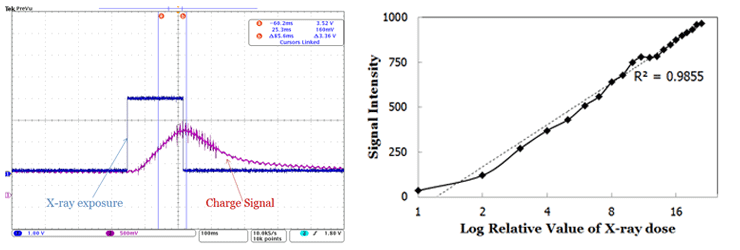
Fig. 4. Output signal of the analog circuit and characteristic curve of PXD system
Figure 4 shows the output signal of the analog circuit (left) and the characteristic curve of the PXD (right) which has been evaluated using Al-wedge phantom. In this experiment, 31-HR-100P (Samil x-ray) mobile x-ray generator was used and its exposure condition was 80 kVp, 20 mA, and 0.1 second. The correlation coefficient and SNR were 0.9855 and 52.9, respectively.
Conclusion and Discussion
In this study, we explored the feasibility of using PXD and detector dedicated electronic circuits. As an imaging detector, the PXD requires a specific charge collection scheme and appropriate electronics. We employed a line-scan technique to obtain a digital radiography image with this detector. The initial performance of PXD and its circuit has been evaluated quantitatively. Since the proposed system still has some components to be improved in order to utilized for DR detector, PXD can replace the conventional DR detector.
Participating Researchers